About the DS200TCDAG1A
This DS200TCDAG1A printed circuit board was originally manufactured to exist as a member of the Mark V Series of turbine control systems, as explained above and in any pertinent General Electric instructional manual materials. This DS200TCDAG1A PCB has an official manual-defined functional product description as a Digital I/O Board, a fact that is reinforced by this DS200TCDAG1A PCB's TCDA functional acronym. This DS200TCDAG1A printed circuit board is not considered the original Digital Input/Output or I/O Board produced for General Electric's Mark V Turbine Control System Series, as it modified the original DS200TCDAG1 parent Digital I/O Board through its inclusion of an A-rated functional product revision.
Hardware Tips and Specifications
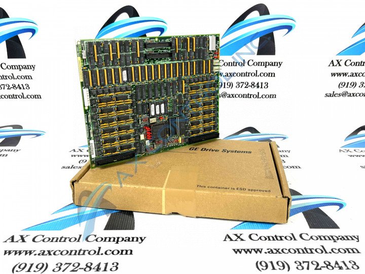
The General Electric DS200TCDAG1A Speedtronic Mark V LM Digital I/O Board is designed to process the digital contact input signals from the corresponding terminal boards in the application, and as such, is befitted with its own series of important and specific hardware components.The General Electric Digital I/O Board DS200TCDAG1A features one microprocessor and multiple programmable read-only memory (PROM) modules. It also contains 1 block made up of 10 LED lights and a pair of 50-pin connectors. The GE Digital I/O Board DS200TCDAG1A also is populated with 8 jumpers and 1 green LED that is visible from the side of the board. These mentioned PROM modules are removable from the board and they reside in a socket embedded on the board. When you want to replace the board or if you want to replace the PROM module for any reason, you can obtain a hand tool that is expressly designed for removing and installing the PROM modules.
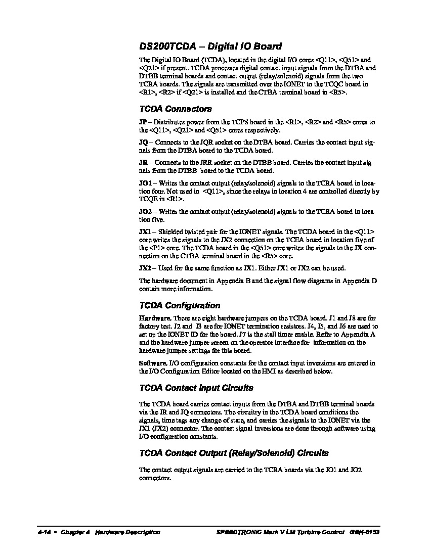
Several important connectors and jumpers exist in the assembly of this DS200TCDAG1A Mark V Series printed circuit board product. For starters, this DS200TCDAG1A Digital I/O Board has eight total significant hardware jumpers, each of which is accompanied by its own factory-printed nomenclature label. The J1 and J8-labeled jumpers in the assembly of this DS200TCDAG1A PCB are for factory testing purposes only. This DS200TCDAG1A PCB's J2 and J3 jumpers are included for the selection of IONET termination resistors. Jumpers J4, J5, and J6 in the assembly of this Mark V Series Digital I/O Board are for the selection of this PCB's IONET ID, while the final J7-labeled jumper in this DS200TCDAG1A PCB's assembly was included for stall timer enable selection. Contact inputs for the related Mark V Series DTBA and DTBB terminal boards interface using this DS200TCDAG1A Digital I/O Board's JR and JQ connectors, only two of the numerous different connector type available to this General Electric Speedtronic-driven product offering. All of the aforementioned hardware component inclusions and set specifications should be protected by this DS200TCDAG1A PCB's thick layer of normal-style PCB protective coating.


