❮


❯


DS200TCDAH1B
- 4.88 (17)
- Click a star to rate this product
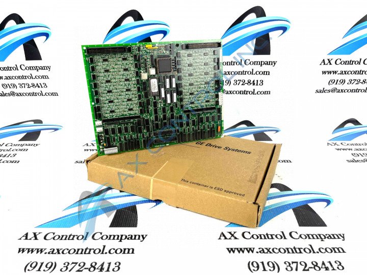
The DS200TCDAH1B General Electric Digital I/O Board was manufactured for use in the Mark V Series of turbine control systems.


* Learn More About Product Conditions
* Posted pricing available for website purchases only.
Product Conditions
New Surplus Factory Package: A completely unused product that is in the original factory package. The package may have been opened for the purpose of pictures, but the product has never been used or installed.
New Surplus AX Control Package: A completely unused product that has been removed from the original factory package. Often due to shelf wear or previous shipping, the factory package is not adequate and must be replaced with an ideal AX Control product package.
Reconditioned: All products that qualify as reconditioned have completed AX Control's thorough and detailed QA process and meet the requirements of excellent working condition and excellent cosmetic condition.
About the DS200TCDAH1B
This DS200TCDAH1B printed circuit board is a well-documented product offering developed as a member of the Mark V Series of turbine control systems, as evidenced by its placement in several relevant Mark V Series instructional manual materials. The Mark V Series that this DS200TCDAH1B product offering belongs to its a relatively recently-developed General Electric product series that utilizes the patented Speedtronic technology that the respected automated industrial retailer has been designing since the introduction of the Mark I in the late 1960s. This DS200TCDAH1B printed circuit board or PCB for short is better-definable as a Digital IO or Digital I/O Board, the original functional descriptions that it possesses in factory-printed General Electric and Mark V Series instructional manual materials. This DS200TCDAH1B PCB is an edited version of the original DS200TCDAH1 Mark V Series Digital IO Board, modifying its parent PCB through the inclusion of a singular B-rated functional product revision.
Hardware Tips and Specifications
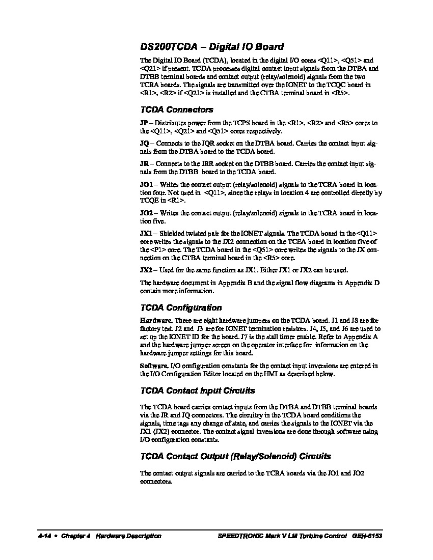
Luckily enough, this DS200TCDAH1B printed circuit board is a well-documented product, for hardware component and specifications identification purposes.The GE Digital I/O Board DS200TCDAH1B features one microprocessor and multiple programmable read only memory (PROM) modules. It also contains 1 block of 10 LEDs and 2 50-pin connectors. The GE Digital I/O Board DS200TCDAGH1B also is populated with 8 jumpers and 1 LED that is visible from the side of the board. The GE Digital I/O Board DS200TCDAH1B also features 2 3-pin connectors. One 3-pin connector has the ID JX1 and the other has the ID JX2. The IDs assigned to the 8 jumpers in this DS200TCDAH1B PCB's assembly are prefixed with JP. For example, one jumper is assigned the ID JP1. Another jumper is assigned the ID JP2, and so on. The jumpers in the assembly of this DS200TCDAH1B printed circuit board are all included to select for a specific DS200TCDAH1B board application. Jumpers J1 and J8 on this DS200TCDAH1B PCB's base circuit board are included for factory testing purposes, and should not be accessed during normative function of the DS200TCDAH1B PCB. Jumpers J2 and J3 included with the DS200TCDAH1B Digital IO Board are intended for IONET Termination Resistors, while this DS200TCDAH1B product's J4, J5, and J6-labeled hardware jumpers select for this device's crucial IONET ID. The final remaining J7 jumper in the assembly of this TCDA-abbreviated printed circuit board was included to select this device's stall timer enable.
The test points in this DS200TCDAH1B Mark V Series product's assembly also have a prefix assigned to the IDs; the prefix for these test points being TP. For example, one test point is assigned the ID TP1, while another test point is assigned the ID TP2. With the use of a qualified testing device, a servicer can test the individual circuits on the board and pinpoint a fault that might be repairable. DS200DTBA and DS200DTBB are other related boards that are installed in the Mark V Series automated drive. Both receive signals from the GE Digital I/O Board DS200TCDAH1B through the 50-pin connectors in this DS200TCDAH1B PCB's internal assembly. One 50-pin connector relevant to this process is assigned ID JQ and the other 50-pin connector is assigned ID JR. Connector JQ connects to the JQR connector on DS200DTBA, with 50-pin ribbon cables providing the signals between the boards. Connector JR receives the contact input signal from DS200DTBB.
DS200TCDAH1B Manuals, White Papers, Data Sheets, and Troubleshooting
DS200TCDAH1B Technical Specifications
| Manufacturer | GE General Electric |
| Series | Mark V |
| Part Number | DS200TCDAH1B |
| Functional Description | Digital I/O Board |
| Functional Acronym | TCDA |
| PCB Coating | Conformal Coating |
| Functional Revision 1 | B |
Frequently Asked Questions about DS200TCDAH1B
What does DS200TCDAH1B do?
What is connector JQ for on DS200TCDAH1B?
Which network does DS200TCDAH1B transmit over?
Reviews For DS200TCDAH1B
Internal Review
(5.0)This DS200TCDAH1B Digital IO, Digital I/O, or Digital Input/Output Board is a crucial member of its greater Mark V Turbine Control System Series automated drive assembly, no matter what you decide to call it. This DS200TCDAH1B Digital IO Board is a supremely-customizable Mark V Series product offering; offering numerous manually-moveable hardware jumpers. The DS200TCDAH1B PCB distinguishes itself further through the inclusion of an exhaustive style of conformal-style printed circuit board protective coating. - AX Control Lead Technician
DS200TCDAH1B Technical Specifications
| Manufacturer | GE General Electric |
| Series | Mark V |
| Part Number | DS200TCDAH1B |
| Functional Description | Digital I/O Board |
| Functional Acronym | TCDA |
| PCB Coating | Conformal Coating |
| Functional Revision 1 | B |
About the DS200TCDAH1B
This DS200TCDAH1B printed circuit board is a well-documented product offering developed as a member of the Mark V Series of turbine control systems, as evidenced by its placement in several relevant Mark V Series instructional manual materials. The Mark V Series that this DS200TCDAH1B product offering belongs to its a relatively recently-developed General Electric product series that utilizes the patented Speedtronic technology that the respected automated industrial retailer has been designing since the introduction of the Mark I in the late 1960s. This DS200TCDAH1B printed circuit board or PCB for short is better-definable as a Digital IO or Digital I/O Board, the original functional descriptions that it possesses in factory-printed General Electric and Mark V Series instructional manual materials. This DS200TCDAH1B PCB is an edited version of the original DS200TCDAH1 Mark V Series Digital IO Board, modifying its parent PCB through the inclusion of a singular B-rated functional product revision.
Hardware Tips and Specifications
Luckily enough, this DS200TCDAH1B printed circuit board is a well-documented product, for hardware component and specifications identification purposes.The GE Digital I/O Board DS200TCDAH1B features one microprocessor and multiple programmable read only memory (PROM) modules. It also contains 1 block of 10 LEDs and 2 50-pin connectors. The GE Digital I/O Board DS200TCDAGH1B also is populated with 8 jumpers and 1 LED that is visible from the side of the board. The GE Digital I/O Board DS200TCDAH1B also features 2 3-pin connectors. One 3-pin connector has the ID JX1 and the other has the ID JX2. The IDs assigned to the 8 jumpers in this DS200TCDAH1B PCB's assembly are prefixed with JP. For example, one jumper is assigned the ID JP1. Another jumper is assigned the ID JP2, and so on. The jumpers in the assembly of this DS200TCDAH1B printed circuit board are all included to select for a specific DS200TCDAH1B board application. Jumpers J1 and J8 on this DS200TCDAH1B PCB's base circuit board are included for factory testing purposes, and should not be accessed during normative function of the DS200TCDAH1B PCB. Jumpers J2 and J3 included with the DS200TCDAH1B Digital IO Board are intended for IONET Termination Resistors, while this DS200TCDAH1B product's J4, J5, and J6-labeled hardware jumpers select for this device's crucial IONET ID. The final remaining J7 jumper in the assembly of this TCDA-abbreviated printed circuit board was included to select this device's stall timer enable.
The test points in this DS200TCDAH1B Mark V Series product's assembly also have a prefix assigned to the IDs; the prefix for these test points being TP. For example, one test point is assigned the ID TP1, while another test point is assigned the ID TP2. With the use of a qualified testing device, a servicer can test the individual circuits on the board and pinpoint a fault that might be repairable. DS200DTBA and DS200DTBB are other related boards that are installed in the Mark V Series automated drive. Both receive signals from the GE Digital I/O Board DS200TCDAH1B through the 50-pin connectors in this DS200TCDAH1B PCB's internal assembly. One 50-pin connector relevant to this process is assigned ID JQ and the other 50-pin connector is assigned ID JR. Connector JQ connects to the JQR connector on DS200DTBA, with 50-pin ribbon cables providing the signals between the boards. Connector JR receives the contact input signal from DS200DTBB.
DS200TCDAH1B Manuals, White Papers, Data Sheets, and Troubleshooting
Frequently Asked Questions about DS200TCDAH1B
What does DS200TCDAH1B do?
What is connector JQ for on DS200TCDAH1B?
Which network does DS200TCDAH1B transmit over?
Reviews For DS200TCDAH1B
Internal Review
(5.0)This DS200TCDAH1B Digital IO, Digital I/O, or Digital Input/Output Board is a crucial member of its greater Mark V Turbine Control System Series automated drive assembly, no matter what you decide to call it. This DS200TCDAH1B Digital IO Board is a supremely-customizable Mark V Series product offering; offering numerous manually-moveable hardware jumpers. The DS200TCDAH1B PCB distinguishes itself further through the inclusion of an exhaustive style of conformal-style printed circuit board protective coating. - AX Control Lead Technician


