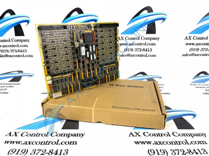
About the DS215TCDAG1BZZ01A
The DS215TCDAG1BZZ01A is a GE Turbine Control Printed Circuit Card. This card is no longer being supported by GE and is now hard to locate, especially given its presence within the now-obsolete Mark V Speedtronic legacy product series. As you can probably tell by the insertion of the Speedtronic in its full series name, the Mark V Series that this DS215TCDAG1BZZ01A product offering belongs to is one of the final General Electric Mark product series to incorporate their patented Speedtronic control system technology into its various offerings. This DS215TCDAG1BZZ01A printed circuit board product offering is not the original device of its functionality developed for the Mark V Turbine Control System Series, as it edits the original DS215TCDAG1 parent circuit board through its adoption of a B-rated significant functional product revision as well as an optional software package. Additionally, this DS215TCDAG1BZZ01A PCB is not considered to be a device with a normal Mark V Series assembly version, as indicated by the presence of the abnormal DS215 series tag at the very beginning of the DS215TCDAG1BZZ01A functional product number. AX Control does try to keep this board in stock as a refurbished or new surplus part.
Hardware Tips and Specifications
The DS215TCDAG1BZZ01A is a Digital I/O Board. The TCDA board can be found within the digital I/O cores <Q11> and <Q51>. It has the power to process output signals coming from the two TCRA boards and the input signals coming from the DTBB and DTBA boards. These signals are then normally sent across the IONET to the terminal board CTBA and the TCQC board. The DS215TCDAG1BZZ01A has several types of connectors that do different things. The JP connector has the ability to transfer power from the TCPS board to the <Q11> and <Q51> cores. The JX1 is a connection for the IONET signals that is a shielded twisted-pair connector. The JX2 connector is also used for IONET signals. The JQ connector goes to the JQR plug on the DTBA board and has the power to ferry signals to the TCDA board. The JO1 link is usually not used with the <Q11> core but in other cores, it is used for communication and can write the contact output signals going to the TCRA board that is in location 4. The JO2 connection can be utilized with the <Q11> and <Q51> cores and the output signals it collects are transcribed to the TCRA board that is positioned in location 5. The JR connection can ferry the input signals that are coming from the DTBB card to the TCDA card. The DTBB board is linked to the JRR socket.
The above connector information is purely reminiscent of a visual inspection of the DS215TCDAG1BZZ01A product itself, paired with our lead service technician's knowledge of standard Speedtronic Mark V Series connections and interfacing potentials. This is the case as this DS215TCDAG1BZZ01A Digital I/O Board or Digital I/O Module's original instructional manual materials are not available in troves on the internet for research purposes. With this in mind, the DS215TCDAG1BZZ01A functional product number itself can be considered a great source of DS215TCDAG1BZZ01A hardware component and component specification information, with functional naming chunks coding for DS215TCDAG1BZZ01A board details including its:
- Special Mark V Series assembly version
- TCDA functional product abbreviation
- Normal PCB coating style
- Group one Mark V Series product grouping
- B-rated primary functional revision
- Optional software package included


